您现在的位置是:主页 > 基础 > 其他基础电路图 >
LinearFM50WattwithBLY9050WFM调频功放电路-其他基础电路图
发布时间:2023-02-08 04:37:36所属栏目:其他基础电路图 已帮助人编辑作者:电路图知识网
Linear FM 50Watt with BLY90 50W FM调频功放电路
A amplifier of force RF for the FM, is always essential for the amateur that wants it strengthens some small transmitter, that likely already it has manufactured or has been supplied ready. The present circuit can give 50-60W RF force of expense, with control smaller than 15-20W in the region of frequencies of FM, that is to say in the 88-108MHZ. Transistor that we selected for this manufacture is the BLY90, that has gain 5dB.
Description
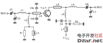
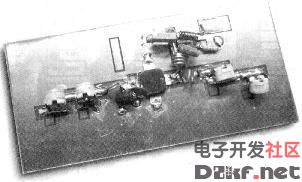
image 1
As it appears in the analytic drawing (image 1) the amplifier is manufactured with transistor TR1, type BLY90 of Philips. The transistor this is specifically drawn for operation in frequencies up to 175MHZ, with very good results of linearity and record of force. In his technical' characteristics they are included the tendency of operation in the 12V the current of collector in the gain expense in the 5dB (measured in order C) and force of entry in the 16W. Variable capacitors C1, C2, with inductor L1, constitute the circuit of co-ordination, that adapts the exit of our transmitter in amplifier RF. This circuit has been calculated suitably, so that it covers all band the FM with the biggest possible output. Inductor RFC1 polarized the transistor, so as to it works in order C, that is to say with the biggest output. Inductor L2 in the collector of TR1, constitutes the charge of amplifier, while RFC2 prevents the RF signals leak in the line of catering. Capacitor C2 and resistance R1, protect the circuit from auto polarization. The coordinated circuit of expense that is constituted by inductor L2 and variable capacitors C3, C4, adapts the exit of amplifier RF with the next stage, which can be constituted from some amplifier RF of high force ( 300W) or a aerial. This circuit can be supplied with 12V f.e from the battery of border=0>
image 2If all they are it includes, you connect the exit of your transmitter (15-20W) in input the amplifier. The exit of amplifier him you will connect in some charge (dummy load) or in the aerial, through bridge stagnant waves. Supply with tendency 11-15V your amplifier (power supply it should gives current 4-5A). Regulate the 4 variable C1-C4, until you take the biggest force of expense. The amplifier is ready.Parts C1-C4 = 10-80pFL1 = 1 coils of diameter of 10mms, 1mmC5 = 10nFL2 = 7 coils of diameter of 10mms, 0,8mmsC6 = 1000pFL3 = 3 coils of diameter of 10mms, 1mmC7 = 100nFTR1 = BLY90C8 = 2200mF/35V
Tags:

相关文章
猜你喜欢

可控硅与场效应管及三极管的区别-其他基础电路图
可控硅与场效应管及三极管的区别 1.场效应管的源极s、栅极g、漏极d分别对应...
CD4071 CD4081中文资料_CD4071功能引脚图_CD4081应用电路图-其他基础电路图
CD4071 四2输入端或门OR NSC/TI CD4081 四2输入端与门AND NSC/HIT/TI CD4071真值表:Y=A+B...
采用RS触发器的防抖电路-其他基础电路图
所示为采用RS触发器的防抖动电路。由图可 知,在开关的触点部位加了RC积分电...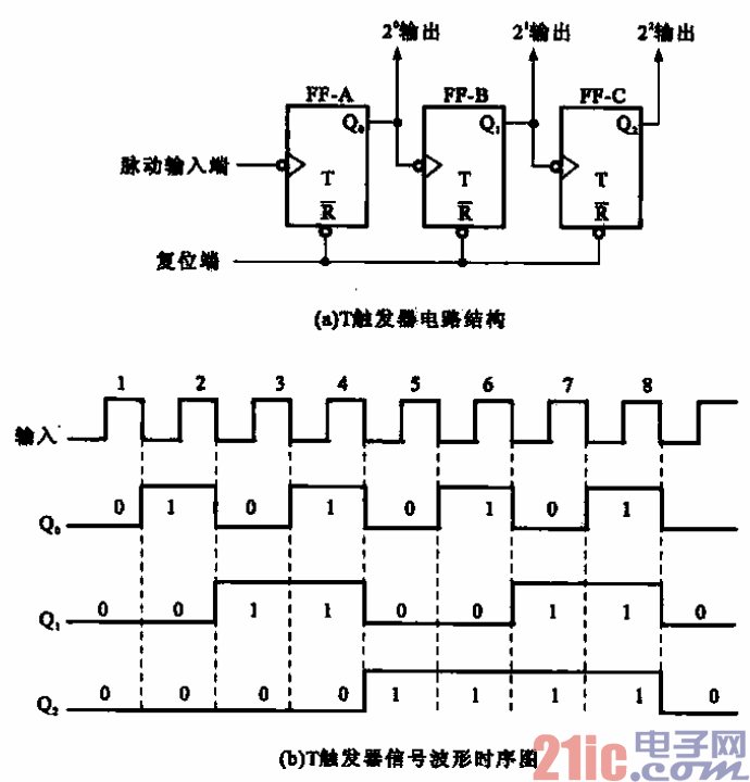
由T触发器组成的非同步即使输球电路及其信号波形-其他基础电路图
所示是利用T触发器组成的计数器电路及其信号波形,它是一种非同步式计数器...

其他基础电路图相关资讯
晶振负载电容的计算-其他基础电路图
可选择带宽的NOTCH滤波器-其他基础电路图
超高频射频识别标签灵敏度的测试方法及解决方案-其他基础电路图
-
电阻器好坏的判断与检测-其他基础电路图
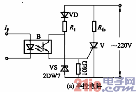
供电耦合器一晶闸管的接口电路a-其他基础电路图
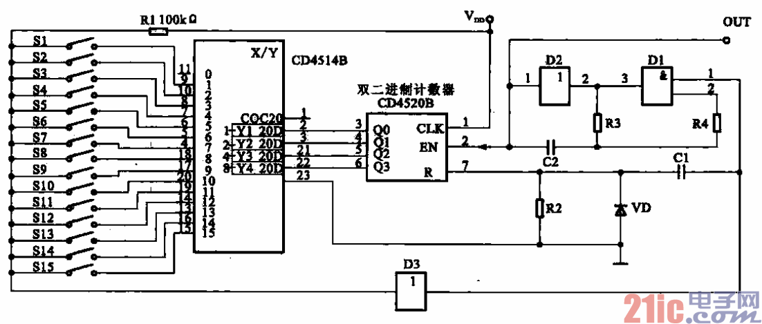
多路脉冲编码器-其他基础电路图
LM7824A中文资料-其他基础电路图
-
提高功率因数的方法-其他基础电路图
CD4027中文资料-其他基础电路图
简易电平转换电路图-其他基础电路图
经典实用的单片机模块电路设计_单片机电路图-其他基础电路图
采用CMOS或非门的防抖动电路-其他基础电路图
稳压用运算放大器基本电-其他基础电路图
具有75欧同辅导线的阻抗-其他基础电路图

焊锡技术-教你怎样使焊锡点光亮-其他基础电路图