您现在的位置是:主页 > 音频 > 其他音频电路图 >
便携式混频器电路PortableMixer-其他音频电路图
发布时间:2022-11-16 03:36:36所属栏目:其他音频电路图 已帮助人编辑作者:电路图知识网
便携式混频器电路 Portable Mixer
Design description:
The target of this project was the design of a small portable mixer supplied by a 9V PP3 battery, keeping high quality performance.
The mixer is formed assembling three main modules that can be varied in number and/or disposition to suit everyone needs.
The three main modules are:
Input Amplifier Module: a low noise circuit equipped with a variable voltage-gain (10 - 100) pre-set, primarily intended as high quality microphone input, also suitable for low-level line input.
Tone Control Module: a three-band (Bass, Middle, Treble) tone control circuit providing unity-gain when its controls are set to flat frequency response. It can be inserted after height=449 src="/data/attachment/portal/201007/ET30794201007221016341.jpg" width=593 border=0>
Input Amplifier Module
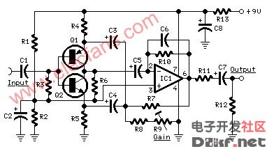
Parts:
R1,R2,R7_______22K 1/4W Resistors
R3,R4,R5_______47K 1/4W Resistors
R6______________4K7 1/4W Resistor
R8,R13________220R 1/4W Resistors
R9______________2K 1/2W Trimmer Cermet (See Notes)
R10___________470K 1/4W Resistor
R11___________560R 1/4W Resistor
R12___________100K 1/4W Resistor
C1____________470nF 63V Polyester Capacitor
C2,C8_________100F 25V Electrolytic Capacitors
C3,C4,C5________22 63V Electrolytic Capacitors
C6_____________47pF 63V Ceramic Capacitor
C7______________47 63V Electrolytic Capacitor
Q1____________BC560C 45V 100mA Low noise High gain PNP Transistor
Q2____________BC550C 45V 100mA Low noise High gain NPN Transistor
IC1___________TL061 Low current BIFET Op-Amp
Circuit description:
The basic arrangement of this circuit is derived from the old Quad magnetic pick-up cartridge module.
The circuit was rearranged to cope with microphone input and a single-rail low voltage supply.
This low-noise, fully symmetrical, two-transistor head amplifier layout, allows the use of a normal FET input Op-Amp as the second gain stage, even for very sensitive microphone inputs.
The voltage-gain of this amplifier can be varied by means of R9 from 10 to 100, i.e. 20 to 40dB.
Notes:
R9 can be a trimmer, a linear potentiometer or a fixed-value resistor at will.
When voltage-gain is set to 10, the amplifier can cope with 800mV peak-to-peak maximum Line levels.
Current drawing for border=0>
Parts:
P1,P2_________100K Linear Potentiometers
P3____________470K Linear Potentiometer
R1,R2,R3_______12K 1/4W Resistors
R4,R5___________3K9 1/4W Resistors
R6,R7___________1K8 1/4W Resistors
R8,R9__________22K 1/4W Resistors
R10___________560R 1/4W Resistor
R11___________100K 1/4W Resistor
R12___________220R 1/4W Resistor
C1______________1F 63V Polyester Capacitor
C2_____________47nF 63V Polyester Capacitor
C3,C5___________4n7 63V Polyester Capacitors
C4_____________22nF 63V Polyester Capacitor
C6,C8_________100F 25V Electrolytic Capacitors
C7______________47 63V Electrolytic Capacitor
IC1___________TL061 Low current BIFET Op-Amp
Circuit description:
This is a straightforward design using the Baxandall-type active circuitry slightly modified to obtain a three-band control. Total voltage gain of this module is 1 when controls are set in their center position.
Notes:
Current drawing for border=0>
Parts:
P1,___________100K Linear Potentiometer
P2_____________10K Linear Potentiometer
R1,R2,_________15K 1/4W Resistors
R3,R4,R11,R12_100K 1/4W Resistors
R5,R6__________22K 1/4W Resistors
R7,R8_________390K 1/4W Resistors
R9,R10________560R 1/4W Resistors
R13___________220R 1/4W Resistor
C1,C2_________330nF 63V Polyester Capacitors
C3,C8_________100F 25V Electrolytic Capacitors
C4,C5__________10pF 63V Ceramic Capacitors
C6,C7___________47 63V Electrolytic Capacitors
IC1___________TL062 Low current BIFET Dual Op-Amp
Circuit description:
The schematic of this circuit is drawn as a stereo unit to better show the input Main Fader and Pan-Pot connections. The TL062 chip contains two TL061 in the same 8 pin case and is wired as two virtual-earth mixer amplifiers having a voltage gain of about 4, to compensate for losses introduced in the passive Pan-Pot circuitry. Therefore, total voltage-gain is 1.
Each channel added to the mixer must include the following additional parts:
P1, P2, R1, R2, R3, R4, C1 and C2.
These parts must be wired as shown in the above circuit diagram, connecting R3 and R4 to pin #2 and pin #6 of IC1 for Right and Left channel respectively. These IC1 pins are the "virtual-earth mixing points" and can sum together a great number of channels.
Notes:
Current drawing for one stereo Main Mixer Amplifier Module is 800A.
Frequency response is 20Hz to 20KHz - 0.5dB.
Total Harmonic Distortion measured @ 2V RMS output = 0.008% @ 1KHz; 0.017% @ 10KHz.
THD is 0.005% @ 1V RMS output.
Maximum undistorted output voltage: 2.8V RMS.
Further Parts:
To parts listed above should be added: one Main on-off SPST switch, a LED used as pilot-light with its dropping 2K2 1/4W series-resistor, DPDT switches to enable or omit Tone Control Modules as shown in the Block diagram, input and output connectors of the type preferred, one stereo dual-gang 100K potentiometer to fade the Stereo Line Input as shown in the Block diagram, battery clip, PP3 9V battery, knobs etc.
Tags:
相关文章

其他音频电路图相关资讯
LA4497nbsp;音响IC电路图-其他音频电路图
用PVC管制成高品质音箱-其他音频电路图
LA4461Namp;nbsp;音响IC电路图-其他音频电路图
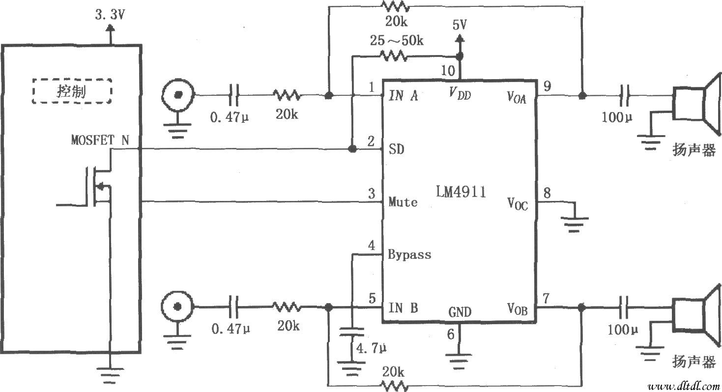
LM4911的不同电源导通时间电路-其他音频电路图
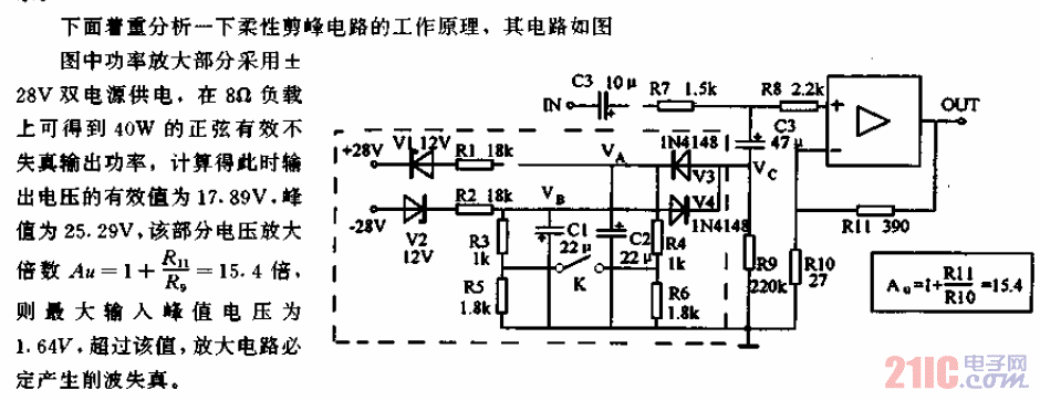
柔性剪峰电路-其他音频电路图

PANASONIC CQ-FX35-55LEN汽车音响电路图-其他音频电路图
-
功放机放音时左右两声道均失真-其他音频电路图
8管OTL耳放的电路图-其他音频电路图
电子蜂鸣器与集成电路NE555定时器-其他音频电路图

电话铃声发生器电路图-其他音频电路图
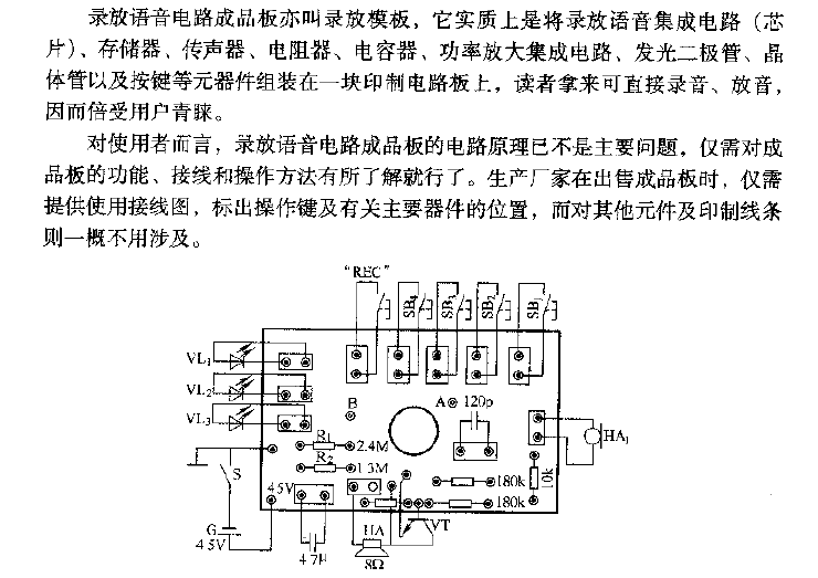
HFC—L5 6s随机录放语音加音乐成品板-其他音频电路图
粉红噪声发生器-其他音频电路图
-
音箱的寿命与保养-其他音频电路图

先锋VSX-D906X/D906S/07TX/09TX功放后级电路图-其他音频电路图
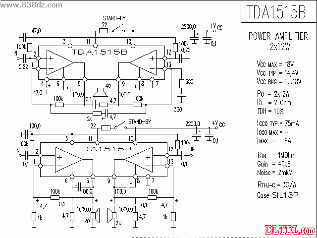
TDA1515B功放电路图纸原理图-其他音频电路图