您现在的位置是:主页 > 信号处理 >
TI MSP432P401R超低功耗混合信号MCU开发方案-信号处理电子电路图
发布时间:2023-01-24 21:15:26所属栏目:信号处理 已帮助人编辑作者:电路图知识网
TI公司的MSP432P401R是基于ARM Cortex-M4的超低功耗混合信号32位MCU,集合了TI MSP430™低功耗DNA,混合信号特性和ARM 32位Cortex-M4 RISC引擎,具有模拟,定时和通信外设等多种特性,工作频率高达48MHz,主要用于工业与自动化如家庭自办动化,烟雾检测器,条码扫描仪,健康健美设备如手表,活动监视器和血糖仪,电表和流量表和消费类电子.本文介绍了MSP432P401R主要特性,功能框图以及MSP432P401R LaunchPad开发板主要特性,框图,电路图,材料清单和PCB设计文件.
The MSP432P401x device family is TI’s latest addition to its portfolio of efficient ultra-low-power mixedsignal MCUs. The MSP432P401x family features the ARM Cortex-M4 processor in a wide configuration of device options including a rich set of analog, timing, and communication peripherals, thereby catering to a large number of application scenarios where both efficient data processing and enhanced low-power operation are paramount.
Overall, the MSP432P401x is an ideal combination of the TI MSP430™ low-power DNA, advance mixedsignal features, and the processing capabilities of the ARM 32-bit Cortex-M4 RISC engine. The devices ship with bundled driver libraries and are compatible with standardized components of the ARM ecosystem.
MSP432P401R主要特性:

MSP432P401R应用:
• Industrial and Automation
– Home Automation
– Smoke Detectors
– Barcode Scanners
• Health and Fitness
– Watches
– Activity Monitors
– Fitness Accessories
– Blood Glucose Meters
• Metering
– Electric Meters
– Flow Meters
• Consumer Electronics
– Mobile Devices
– Sensor Hubs

图1. MSP432P401R功能框图
MSP432P401R LaunchPad开发板
The MSP432P401R LaunchPad enables you to develop high performance applications that benefit from low power operation. It features the MSP432P401R – which includes a 48MHz ARM Cortex M4F, 95uA/MHz active power and 850nA RTC operation, 14-bit 1MSPS differential SAR ADC and AES256 accelerator.
This Launchpad includes an on-board emulator with EnergyTrace+ Technology, which means you can program and debug your projects without the need for additional tools, while also measuring total system energy consumption.
All pins of the MSP-EXP432P401R device are fanned out for easy access. These pins make it easy to plug in 20-pin and 40-pin BoosterPacks that add additional functionality like wireless, capacitive touch and more.
The out-of-box provided with the MSP-EXP432P401R LaunchPad features a graphical user-interface that enables the user to type in the desired beats per minute of an RGB LED, and select from over 16 million color options. See how simple it is to get started, with the MSP432 Quick Start Guide.
MSP432P401R LaunchPad开发板主要特性:
Low-power, high performance MSP432P401R MCU
48MHz 32-bit ARM Cortex M4F with Floating Point Unit and DSP acceleration
Power consumption: 95uA/MHz active, and 850nA RTC standby operation
Analog: 24Ch 14-bit differential 1MSPS SAR ADC, Two Comparators
Digital: Advanced Encryption Standard (AES256) Accelerator, CRC, DMA, HW MPY32
Memory: 256KB Flash, 64KB RAM
Timers: 4 x16-bit, and 2 x 32-bit
Communication: Up to 4 I2C, 8 SPI, 4 UART
40 pin BoosterPack Connector, and support for 20 pin BoosterPacks
Onboard XDS-110ET emulator featuring EnergyTrace+ Technology
2 buttons and 2 LEDs for User Interaction
Back-channel UART via USB to PC
The MSP432P401R is the first MSP432 family device featuring low-power performance with an ARM Cortex-M4F core. Device features include:
• Low-power ARM Cortex-M4F MSP432P401R
• Up to 48-MHz system clock
• 256KB flash memory, 64KB SRAM, and 32KB ROM with MSPWare libraries
• Four 16-bit timers with capture/compare/PWM, two 32-bit timers, and RTC
• Up to eight serial communication channels (I2C, SPI, UART, and IrDA)
• Analog: 14-bit SAR ADC, capacitive touch, comparator
• Digital: AES256, CRC, uDMA
What’s Included
1 x MSP-EXP432P401R LaunchPad Development Kit
1 x Micro-USB cable
1 x Quick Start Guide

图2.MSP-EXP432P401R LaunchPad开发板外形图
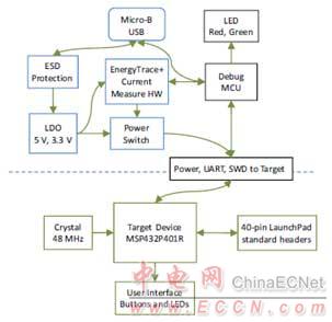
图3.MSP-EXP432P401R LaunchPad开发板框图

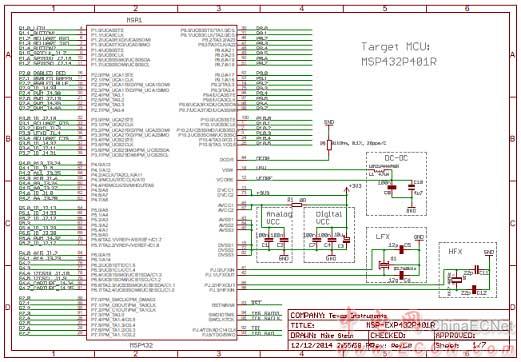
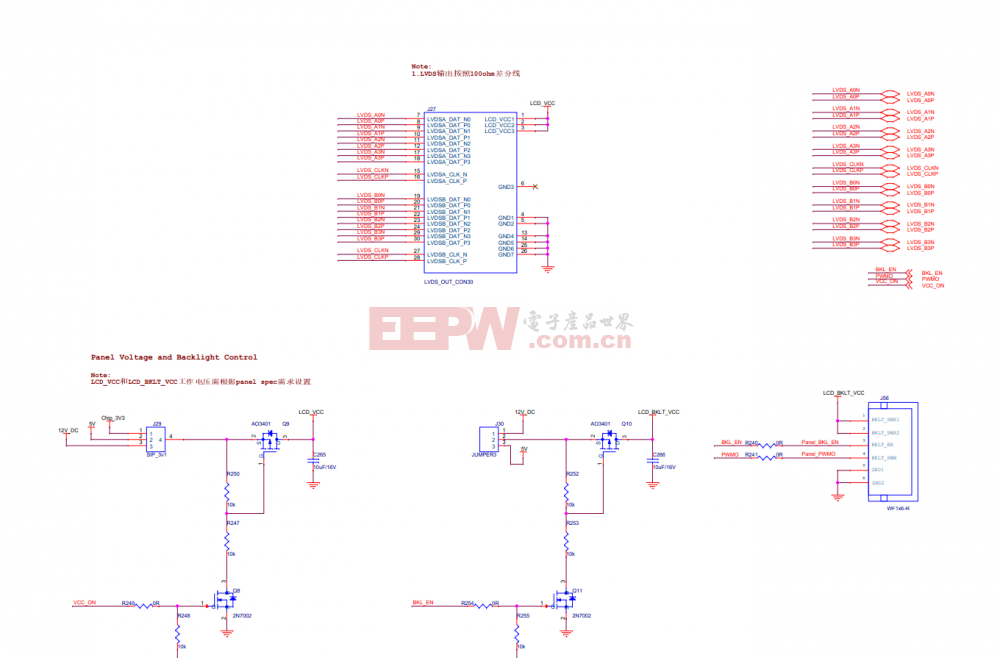
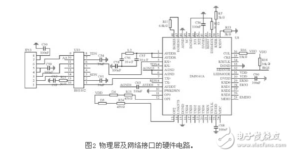
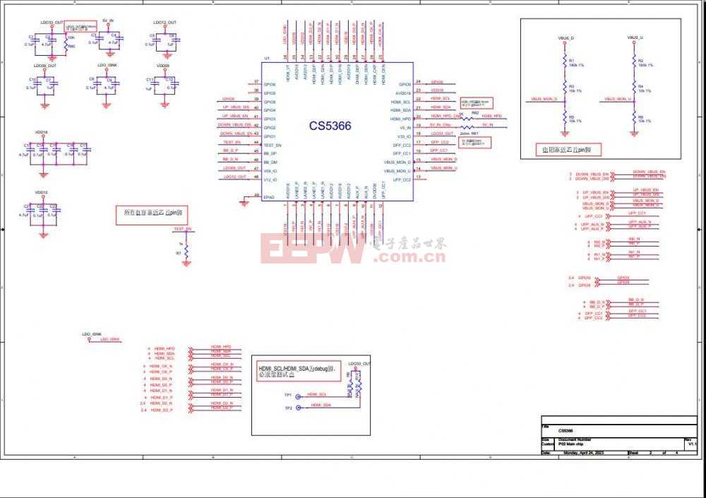
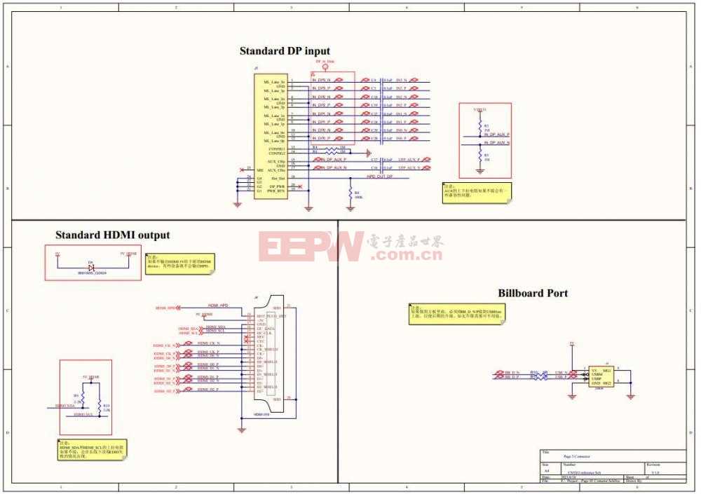
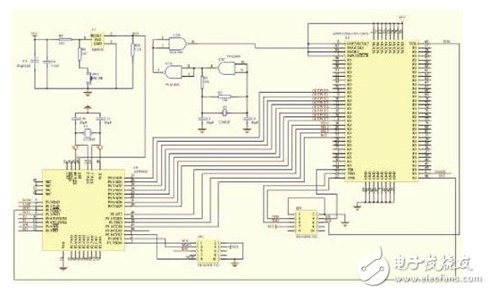
图5.MSP-EXP432P401R LaunchPad开发板电路图(1)

图6.MSP-EXP432P401R LaunchPad开发板电路图(2)
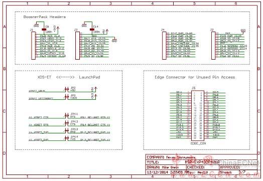
图7.MSP-EXP432P401R LaunchPad开发板电路图(3)

图8.MSP-EXP432P401R LaunchPad开发板电路图(4)
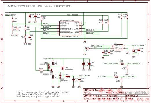
图9.MSP-EXP432P401R LaunchPad开发板电路图(5)

图10.MSP-EXP432P401R LaunchPad开发板电路图(6)
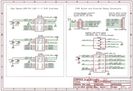
图11.MSP-EXP432P401R LaunchPad开发板电路图(7)
Tags:
相关文章
- 基于ZigBee协议的无线通讯硬件电路设计图-信号处理电子电路图
- 具有调零及满度功能的信号处理电子电路图-信号处理电子电路图
- 信号机电路图讲解和实物图(黄灯点灯电路/出站信号机点灯/进站信号机点灯电路)-信号处理电子电路图
- 采用ADAS3023同步数据采集系统电路 —电路图天天读(37)-信号处理电子电路图
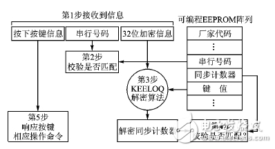
- 无线遥控信号处理电路设计详解-信号处理电子电路图
- 以太网收发电路设计方案详解-信号处理电子电路图
- 智能照明系统室内环境光采集电路图-信号处理电子电路图
- 智能电表中的RS485的通讯模块电路设计-信号处理电子电路图
- 串联和并联反馈放大电路图-信号处理电子电路图
- 解读多间隔脉冲信号连接器电路-信号处理电子电路图
猜你喜欢
CS5511国产DP转LVDS/eDP方案设计电路图-信号处理电子电路图
CS5511是一款适用于低成本显示系统的灵活配置的DP/eDP到LVDS/eDP转换器。CS5511原理...
时钟有回沟?什么原因会导致信号波形边沿的回沟?-信号处理电子电路图
什么原因会导致信号波形边沿的回沟? 信号传输过程中遇到阻抗不连续会产生...
反相加法运算电路,反相积分运算电路(含分析和计算公式)-信号处理电子电路图
集成运算放大器是一种高增益的直流放大器。它有两个输入端,一个输出端。...
TYPEC转HDMI 8K30HZ+USB3.0+PD100W扩展方案CS5466芯片原理图-信号处理电子电路图
CS5466芯片原理图,CS5466单芯片集成Type-C转HDMI8K30HZ或者4K144HZ方案芯片, TYPEC转...

信号处理相关资讯
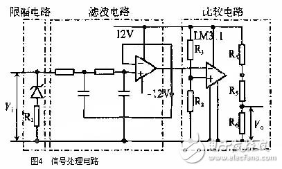
汽车传感器之信号处理电路设计-信号处理电子电路图
电压和电流反馈放大电路图-信号处理电子电路图
解读ZigBee无线终端温度测试系统电路 —电路图天天读(85)-信号处理电子电路图
-
CS5511国产DP转LVDS/eDP方案设计电路图-信号处理电子电路图
微压力传感连接器电路设计详解-信号处理电子电路图
基于CO2128的网络信号转换系统电路设计-信号处理电子电路图
射频无线门禁系统电路设计方案详解 —电路图天天读(114)-信号处理电子电路图
基于NFC通用读卡器电路设计 —电路图天天读(42)-信号处理电子电路图
无线智能照明控制系统电路详解-信号处理电子电路图
ASL CS5466设计TYPEC转HDMI 8K高清扩展投屏方案芯片电路-信号处理电子电路图
CS5263电路原理图|替代IT6561芯片电路|DP转HDMI芯片方案设计-信号处理电子电路图
一种电话语音信号光纤接收机电路设计-信号处理电子电路图
用D-CAP模式的TPS53355芯片如何设计RCC纹波电路-信号处理电子电路图
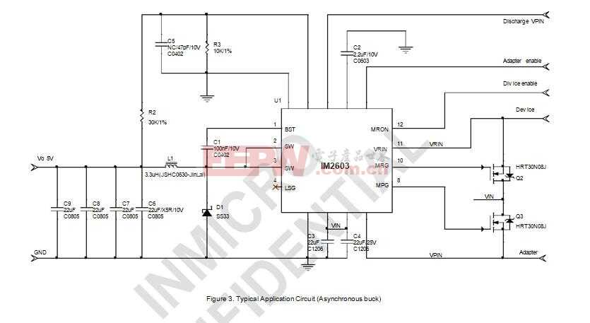
IM2603替代MT3905升降压MOS电源芯片-信号处理电子电路图
采用QCM传感器的差频与控制电路设计-信号处理电子电路图