您现在的位置是:主页 > 通信 > 通信综合电路图 >
Avago ALM-1812高增益GPS前端方案 -通信综合电路图
发布时间:2022-09-17 08:33:42所属栏目:通信综合电路图 已帮助人编辑作者:电路图知识网
Avago公司的ALM-1812是高增益低噪音GPS前端放大器,组合了高增益LNA和GPS FBAR滤波器.LNA采用Avago的GaAs增强模式pHEMT工艺,而一流的FBAR滤波器在Cell/PCS频段有极好的抑制特性,大于85dB. ALM-1812的增益为19.1dB,NF为1.66dB,IIP3 = +2 dBm, IP1dB = -8 dBm.本文介绍了ALM-1812主要特性和指标, 应用电路,演示板布局和电路图以及所用元器件与散射参数和测试参考平面图.
ALM-1812: High-Gain GPS Low Noise Amplifier with Integrated Filters and Variable Current/Shutdown Function
Avago Technologies’ ALM-1812 is a GPS front-end module that combines a high-gain low-noise amplifier (LNA) with GPS FBAR filters. The LNA uses Avago Technologies’ proprietary GaAs Enhancement-mode pHEMT process to achieve high gain with very low noise figure and high linearity. Noise figure distribution is very tightly controlled. A CMOS-compatible shutdown pin is included either for turning the LNA on/off, or for current adjustment. The integrated filter utilizes an Avago Technologies’ leading-edge FBAR filter for exceptional rejection at Cell/PCS-Band frequencies.
The low noise figure and high gain, coupled with low current consumption make it suitable for use in critical low-power GPS applications or during low-battery situations.
ALM-1812主要特性:
• Very Low Noise Figure
• Exceptional Cell/PCS-Band rejection
• Low external component count
• Fully-matched at RF input and RF output
• Shutdown current: 1 uA
• CMOS compatible shutdown pin (SD)
• ESD:> 3kV at RFin pin
• 4.5 x 2.2 x 0.95 mm3 size
• Adjustable bias current via single external resistor/voltage
• Lead-free, Halogen free and meets MSL3
ALM-1812主要指标:
Specifications (Typical performance @ 25°C) At 1.575GHz, Vdd = 2.8V, Idd = 6.8mA
• Gain = 19.1 dB
• NF = 1.66 dB
• IIP3 = +2 dBm, IP1dB = -8 dBm
• S11 = -10 dB, S22 = -15 dB
• Cell-Band Rejection:> 90dBc
• PCS-Band Rejection:> 85dBc
ALM-1812应用:
• GPS Front-end Module

图1. ALM-1812应用电路

图2.ALM-1812演示板布局图
应用电路所用元件表:


图3.ALM-1812演示板和应用电路框图
Notes
1. The module is fully matched at the input and output RF pins. The RFin pin is directly connected to a shunt inductor that is grounded. The RF output filter blocks DC. Best noise performance is obtained using high-Q wirewound inductors. This circuit demonstrates that low noise figures are obtainable with standard 0402 chip inductors.
2. C2 and L2 form a matching network that affects the frequency response and linearity of the LNA, these can be tuned to optimize gain and return loss.
3. L1 and R1 isolates the demoboard from external disturbances during measurement. It is not needed in actual application. Likewise, C1 and C3 mitigate the effect of external noise pickup on the Vdd and Vsd lines respectively. These components are not required in actual operation.
4. Bias control is achieved by either varying the Vsd voltage with/ without R2, or fixing the Vsd voltage to Vdd and adjusting R2 for the desired current.

图4.ALM-1812散射参数和测试参考平面图
Tags:
相关文章


通信综合电路图相关资讯

基于Android平台的即时通信系统客户端设计-通信综合电路图
大时钟,小基站,一颗芯片满足微基站不同外设的时钟需求-通信综合电路图
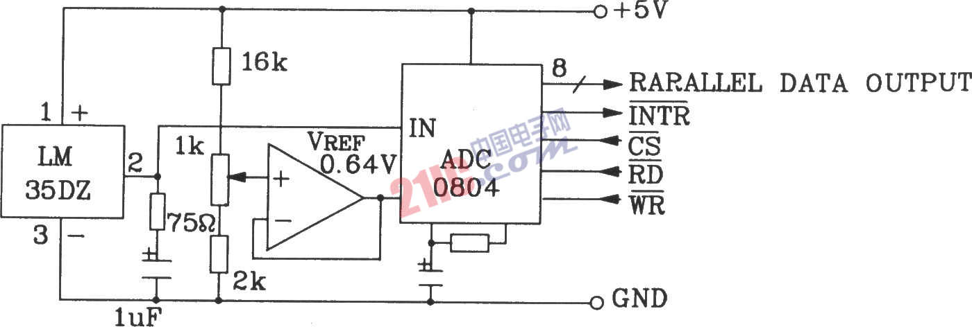
LM35DZ构成并行三态输出标准微机电路-通信综合电路图
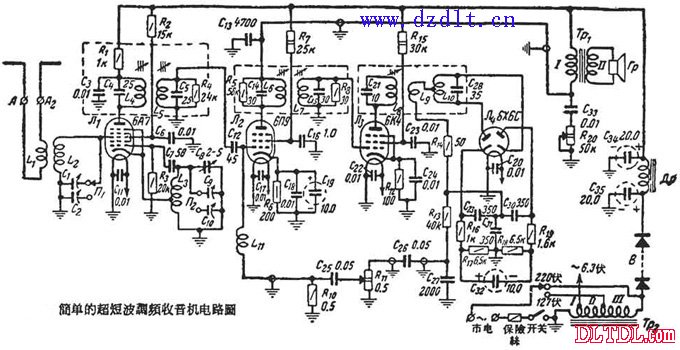
超短波调频收音机电路图-通信综合电路图

基于软件无线电的通信系统试验平台的设计实现,软硬件原理、架构-通信综合电路图

12x10G带宽的可插拔光纤收发器模块,链路距离300米-通信综合电路图
LM386应用于收音机中的电路-通信综合电路图
用于智能标签的运动感知薄型低功耗蓝牙信标解决方案-通信综合电路图
RS-232/485/422单模单纤解决方案-通信综合电路图
电源滤波去耦网络的应用-通信综合电路图
收音机动态调试-通信综合电路图
压缩感知技术在未来移动通信系统中的应用-通信综合电路图
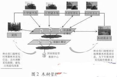
物联网技术在木材管理领域的应用-通信综合电路图
LTE/LTE-A系统自组织网络技术和标准化进展-通信综合电路图
三网融合传输网络解决方案-通信综合电路图