您现在的位置是:主页 > 光电 > 其他光电实用电路图 >
Dual,Voltage-OutputDACConsumesMinisculePower-其他光电实用电路图
发布时间:2023-04-23 16:24:57所属栏目:其他光电实用电路图 已帮助人编辑作者:电路图知识网
Dual, Voltage-Output DAC Consumes Miniscule Power
The dual, voltage-output DACs shown in the figure below employ a combination of power-conserving tricks to draw less than 20µA from a 5V supply. The circuit suits a need for programmable voltage generation in slow or static applications, such as the nulling of offsets in a micropower instrument.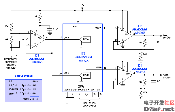
Providing two independent 8-bit DACs with voltage outputs and a common reference, this dual-DAC circuit draws less than 20µA from a 5V supply.
Current-output DACs normally waste power by routing the complement of IOUT to ground. The circuit in the figure avoids wasting power by operating each DAC in the reverse voltage-switching mode, in which the reference voltage is applied to the pins normally labeled IOUT.
The OUT pins in this circuit have a constant and relatively low input impedance of 11kΩ. To reduce input currents, the reference voltage is divided by 100 (from 5V to 50mV) and therefore delivers only 5µA to each DAC input. Signal levels are restored by a compensating gain of 100 in each output amplifier. Inexpensive 10MΩ/100kΩ resistor networks are a good choice for the multiple 100:1 attenuators required. Though only 2% accurate, their matching and tracking is much better than that of discrete resistors.
Greater scaling is impractical because of 0.5mV (maximum) offsets in the output amplifiers shown. Amplified by 100, these offsets produce worst-case output errors of ±1% (0.05V). The errors are constant over temperature, but additional error due to drift over a range of 40°C is typically ±½LSB. The micropower output amplifiers shown in the figure were chosen for their low supply current—their typical IDD is only 1µA.
The last requirement for minimizing the overall current drain is to ensure that logic signals applied to the digital inputs of IC1 swing to within 0.2V of each rail. The maximum specified IDD for that condition is 100µA over temperature, but this specification (like most CMOS IDD ratings) is extremely conservative. IDD is negligible for Rail-to-Rail swings but rises dramatically as the swings approach TTL levels.
A similar version of this article appeared in Electronic Design magazine.
MAX406, MAX407, MAX409 pdf datasheet (单电源运算放大器) MX7528, MX7628 pdf datasheet (双路缓冲驱动8位乘法DAC)
Tags:
相关文章


其他光电实用电路图相关资讯
用PROG-110设计制作的多媒体投影机自动控制器-其他光电实用电路图

用6N7P电子管制作的单端功率放大器-其他光电实用电路图
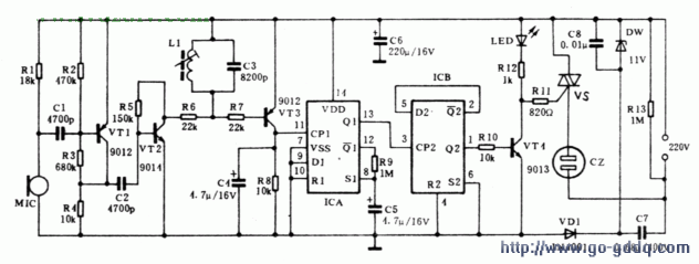
选频声控开关电路设计与分析-其他光电实用电路图
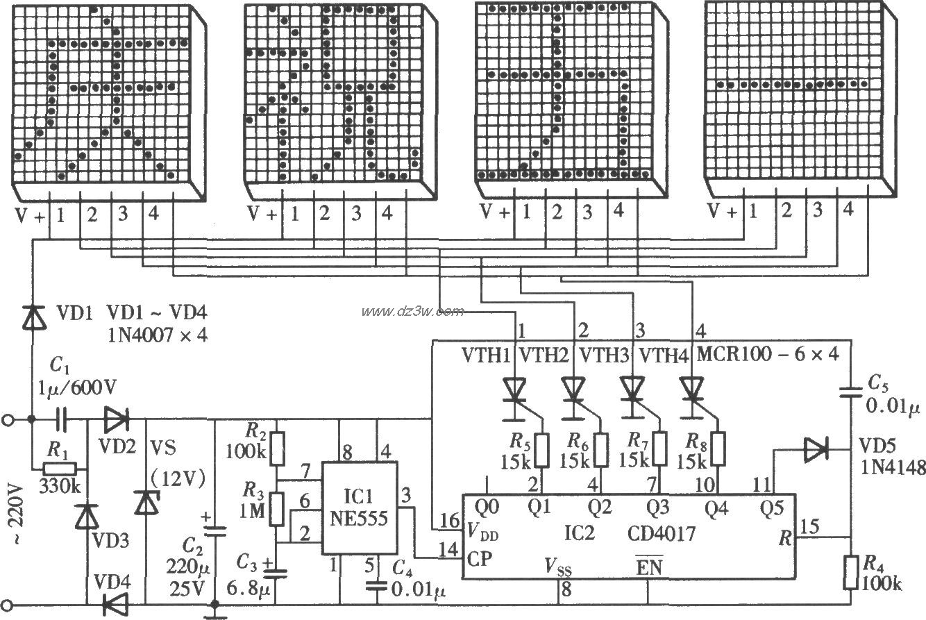
由NE555、CD4017组成的节-其他光电实用电路图
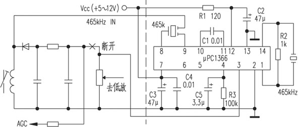
用μPC1366提高收音机灵敏度-其他光电实用电路图
对讲机发射功率测试笔的制作-其他光电实用电路图
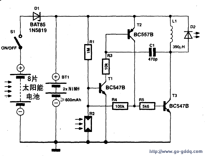
庭院太阳能照明灯电路-其他光电实用电路图
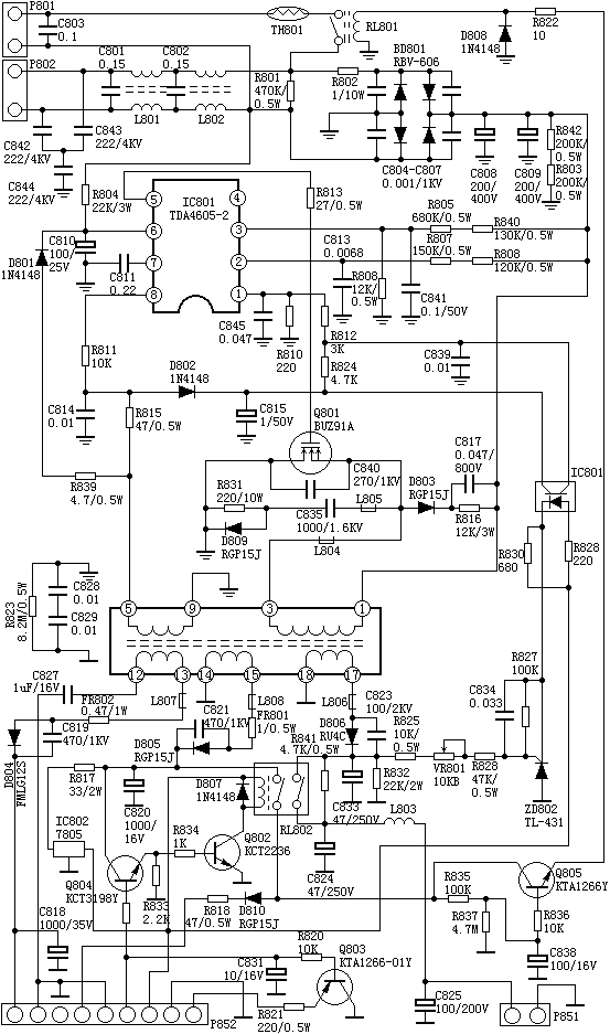
采用TDA4605-2制作的开关电源-其他光电实用电路图
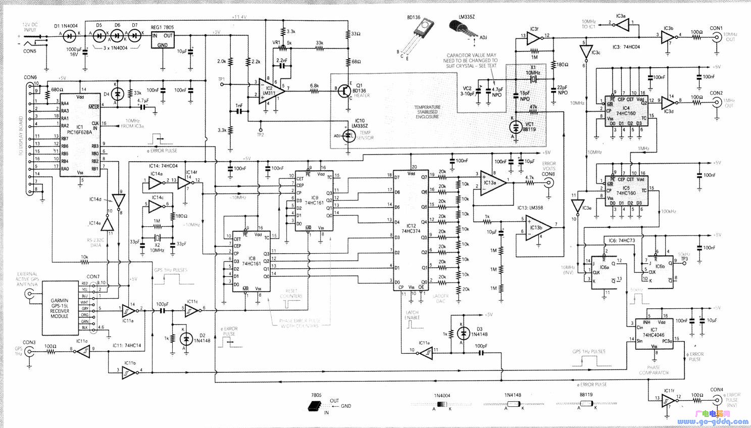
基于定位系统基准频率源的设计与制作-其他光电实用电路图
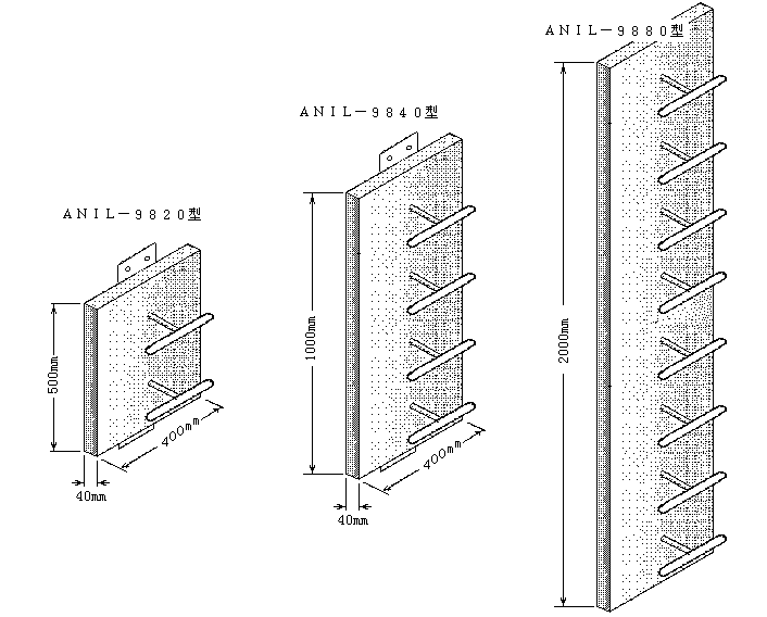
9800系列UHF发射单元的制作方法-其他光电实用电路图
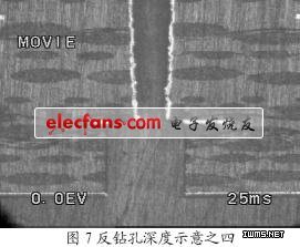
微波多层板反钻孔之金属化孔互连-其他光电实用电路图
卡拉OK人声增效电路-其他光电实用电路图

选择性去桥连技术提高焊接成品率-其他光电实用电路图
电子扩音机安装后的电压检测与调整-其他光电实用电路图
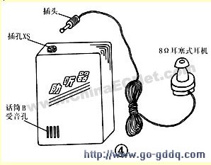
用分立元件制作的耳聋助听器-其他光电实用电路图